 |
Production of strip and multilayer printed circuit boards
Installation of electronic products (IEP) on printed circuit boards and soldering of assembled printed
circuit assemblies are the main operations in the production of modern electronic equipment (REA),
which determine the quality and reliability of the equipment as a whole.
Part number:
Supplier:
JSC SozvezdieDescription
JSC Concern Sozvezdiye
About the product
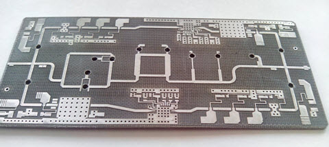
DESCRIPTION
- The maximum number of layers-16, at the stage of working out 24 layers;
- Minimum conductor width / gap on outer layer-0.1/0.1 mm;
– The minimum width of the conductors on the inner layer is 0.075 mm;
- Minimum diameter of through transition holes-0,2 mm at the ratio of Board thickness to hole
diameter-10:1;
- Diameter of "blind" holes-0,3...0,15 mm at the ratio of depth to diameter of a hole-0,8 :1;
– Metallization of the end faces and grooves;
- The maximum thickness of the WFP - 6 mm;
- The minimum thickness of the WFP layer is 0.1 mm;
- Base workpiece size 457 x 305 mm;
- Circuit coating-immersion gold and OS 61 with reflow;
- Liquid photo-proofing solder mask;
- Base materials FR4, RO 4003, RO 4350;
- WFP rectangular and round shape;
- Manufacture of multilayer printed circuit boards 4-5 accuracy class with elements of 6 accuracy class:
About the product
DESCRIPTION
- The maximum number of layers-16, at the stage of working out 24 layers;
- Minimum conductor width / gap on outer layer-0.1/0.1 mm;
– The minimum width of the conductors on the inner layer is 0.075 mm;
- Minimum diameter of through transition holes-0,2 mm at the ratio of Board thickness to hole
diameter-10:1;
- Diameter of "blind" holes-0,3...0,15 mm at the ratio of depth to diameter of a hole-0,8 :1;
– Metallization of the end faces and grooves;
- The maximum thickness of the WFP - 6 mm;
- The minimum thickness of the WFP layer is 0.1 mm;
- Base workpiece size 457 x 305 mm;
- Circuit coating-immersion gold and OS 61 with reflow;
- Liquid photo-proofing solder mask;
- Base materials FR4, RO 4003, RO 4350;
- WFP rectangular and round shape;
- Manufacture of multilayer printed circuit boards 4-5 accuracy class with elements of 6 accuracy class: