 |
THE TECHNOLOGY OF HIBRID-INTEGRATED MICROWAVE CIRCUITS
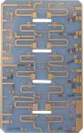
The Corporation has a 30-year experience of development and production of thin-film microstrip boards and microwave HICs based on them.
High-reliable unified technology supported by corresponding standards provides the output of reliable and qualitative production
Part number:
Supplier:
The Ruselectronics holding companyDescription
The complete cycle of technological processes - automated design and mask manufacturing, vacuum (resistive, electron-beam, magnetron) coating of conductive and resistive films, precision photolithography, laser precision hole drilling and dimensional processing of substrates, chemical metallization of holes and halvanic build-up of Cu, Ni, Au layers, precision cutting of substrates with diamond discs – provides about 10000 microstrip boards a month of more than 100 types-dimensions with the following main characteristics:
the substrate material – polycor, ferrite-garnet, quartz
metallization structure of conducting layers: Cr, Cu, Ni, Au; Ti, Pd, Au
Minimal line dimensions – 20 μm, accuracy ±1.5 μm
Minimal diameter of metallized holes – 0.15 mm
Attenuation coefficient (loss) in the strips at 8 GHz frequency is 8 dB/m
Lines for assembling and testing of HICs and microwave modules include: microsoldering of active and passive component chips, microwelding (contact, thermocompression, ultrasonic. thermosonic), module assembling, thermal degassing, microwave module sealing, test on influence of destabilizing factors, provide the output of more than 5000 microwave modules a year